Preparation of SiO2 thin film by Photo-Chemical Vapor Deposition and application in MSM-structured Ultraviolet Photodetectors
|
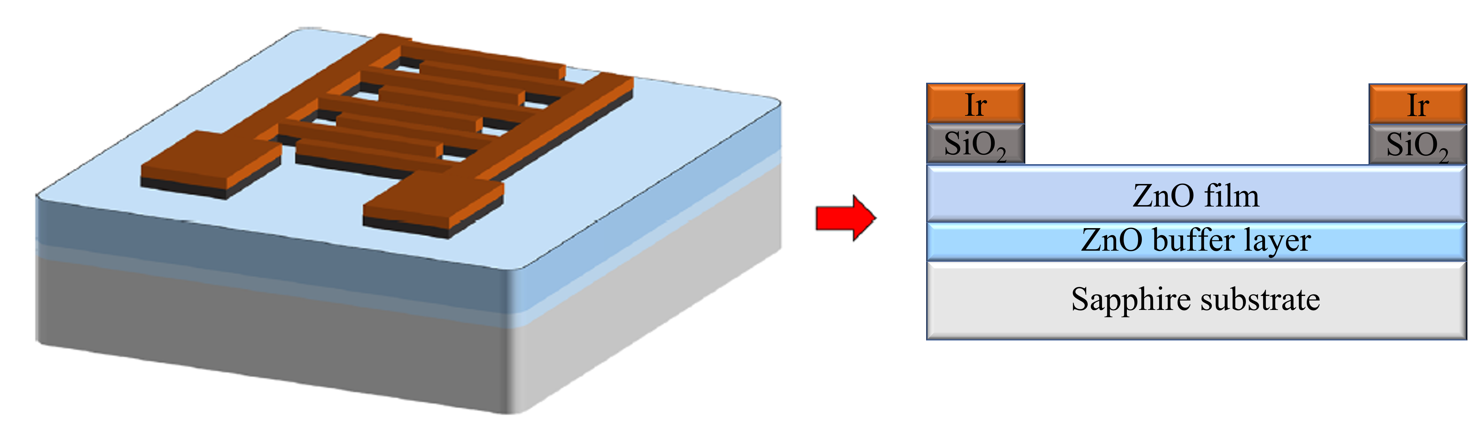
Preparation of SiO2 thin film by Photo-Chemical Vapor Deposition and application in MSM-structured Ultraviolet Photodetectors Ultraviolet (UV) photodetectors (PDs) have been widely used in daily life, whether in the field of electronics, environmental detection, etc. It is very important that the photo-dark current ratio, sensitivity of photo-response and noise analysis of devices were discussed for photodetector. Renally, many research groups have studied the metal−semiconductor−metal (MSM) structure of UV PDs. To improve the performance of the MSM structure photodetectors, it can be improved the performance by an insulating layer inserted between the electrode and the active layer. In the study, it was used photo-chemical vapor deposition to prepare high-quality silicon dioxide as an insulating layer, and the ZnO epitaxial thin film was prepared by RF magnetron sputtering method to fabricate high-performance ultraviolet photodetector. |
|||||||
| _______________________________________________________________________________________________ | |||||||
|
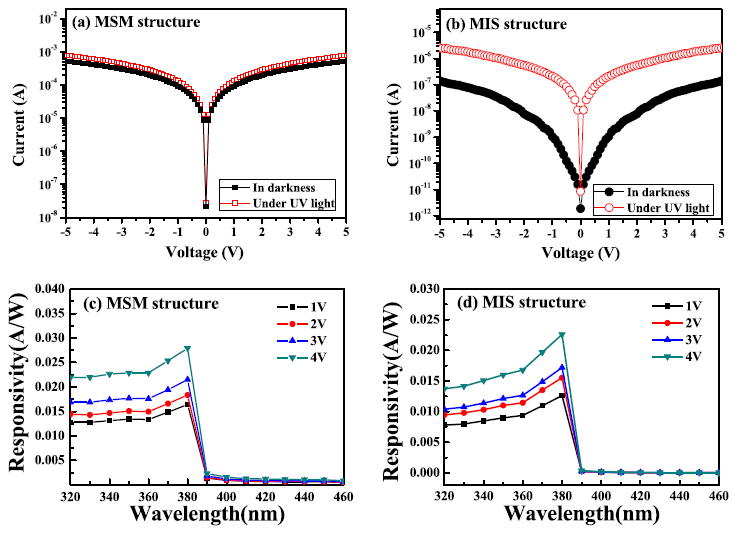
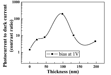
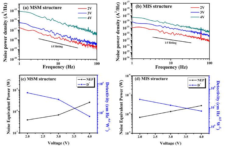
UV PDs have been widely used in daily life, such as electronic equipment, environmental monitors [1-4]. Wide bandgap material, such as SiC, Ga2O3, GaN, TiO2, ZnO have been received the scientist attention in recent years. Among them, ZnO has excellent chemical stability and good optical properties [5-7]. Therefore, it is often used in optical sensors and chemical sensors (such as gas sensors and biosensors). For PD, the photo-dark current ratio, the sensitivity of the photo-response and the noise analysis are often discussed index. Renally, many research groups have studied the metal−semiconductor−metal (MSM) structure of UV PDs. To improve the performance of the MSM structure PDs, it can be improved the performance what by an insulating layer (Al2O3, SiO2, Si3N4, etc) inserted between the electrode and the active layer [8-14]. SiO2 film is the easiest to prepare in these materials by PECVD or sputter method. However, the deposition film quality is not ideal. To improve the quality of SiO2 film, the study was used photo-CVD system to prepare the SiO2 film. The principle mainly uses vacuum ultraviolet light as the light source (deuterium lamp) to effectively excite the synthesis gas in the process of depositing SiO2, and then prepare a high-quality insulating layer. Therefore, this study uses photo-chemical vapor deposition to prepare high-quality SiO2 thin films and applied to the ZnO PD. Figure 1 shows the I-V characteristic curves and photoresponse measurement results of MSM and MIS structure ZnO PDs. The dark and photo currents of the ZnO based MSM structure were 9.23 × 10⁻⁵ and 1.35 × 10⁻⁴. After depositing the SiO2 film, the dark current (1.05× 10⁻⁹ A) decrease significantly about 3~4 order, and the photo current (2.1 × 10⁻⁷) also decrease about 2~3 order. After calculating the ratio of photo to dark current, the ratio of MSM structure was 1.46 and MIS structure was 200 when applied bias at 1V. Deposition of an insulating layer on the ZnO MSM structure not only improves sensitivity but also reduces overall power consumption. On the other hand, the thickness of the insulating layer will also directly affect the performance of the photosensor. In Figure 2, we deposited five different thickness (22, 45, 98, 132, 198 nm) of the SiO2 film to discuss the photoelectric properties difference for ZnO photodetectors. The result shown that all data were significantly improved compared with the non-insulating layer, and the best results can be obtained when the thickness is 98 nm. These results To confirm the trap distribution between the electrode and active layer, we measured the noise power spectra from 1 to 100 Hz in the ZnO-based PDs with MSM and MIS structures in figure 3. The measurement parameters included the varied bias voltages from 2 to 4 V in the dark environment. The noise spectral density was analyzed by Hooge-type equations [15]. When the bandwidth was at the maximum measurement frequency (100 Hz) with an applied bias of 2 V, the NEP and D* values of the MSM structure were 4.082 × 10⁻⁷ W and 4.9 × 106 cm·Hz−0.5·W−1, respectively. When a silicon oxide layer was inserted, the NEP and D* of the device (MIS structure) reached 6.826 × 10⁻⁹ W and 2.93 × 107 cm· Hz−0.5·W−1, respectively. These phenomena indicate the good performance of the insulating layer for PDs. The results show that inserting an insulating layer between the semiconductor and electrode can improve the performance of PDs.
|
|||||||
|
Figure 1 Photoresponse performance of ZnO-based MSM and MIS structure PDs. (a, b) I-V characteristics, (c, d) Responsivity characteristics.
Figure 2 Photocurrent to dark current contrast ratios of PDs with different silicon oxide film thicknesses.
Figure 3 Noise characteristics of ZnO-based MSM and MIS structures operated at various applied biases. (a, b) Noise power density; (c, d) NEP and D*. [1]Sugumar, R.; Angappane, S. Influence of substrate heating and annealing on the properties and photoresponse of manganese doped zinc oxide thin films. Superlattices Microstruct. 2017, 110, 57−67. [2]Shaikh, S. K.; Ganbavle, V. V.; Mohite, S. V.; Rajpure, K. Y. Chemical synthesis of pinecone like ZnO films for UV photodetector applications. Thin Solid Films 2017, 642, 232−240. [3]Kar, J. P.; Das, S. N.; Choi, J. H.; Lee, Y. A.; Lee, T. Y.; Myoung, J. M. Fabrication of UV detectors based on ZnO nanowires using silicon microchannel. J. Cryst. Growth 2009, 311, 3305−3309. [4]Dhar, S.; Majumder, T.; Mondal, S. P. Phenomenal improvement of external quantum efficiency, detectivity and responsivity of nitrogen doped graphene quantum dot decorated zinc oxide nanorod/polymer schottky junction UV detector. Mater. Res. Bull. 2017, 95, 198−203. [5]Mamat, M. H.; Khusaimi, Z.; Zahidi, M. M.; Mahmood, M. R. Performance of an Ultraviolet Photoconductive Sensor Using Well-Aligned Aluminium-Doped Zinc-Oxide Nanorod Arrays Annealed in an Air and Oxygen Environment. Jpn. J. Appl. Phys. 2011, 50, 4. [6]Gahtar, A.; Rahal, A.; Benhaoua, B.; Benramache, S. A comparative study on structural and optical properties of ZnO and Al-doped ZnO thin films obtained by ultrasonic spray method using different solvents. Optik 2014, 125, 3674−3678. [7]Mondal, S.; Bhattacharyya, S. R.; Mitra, P. Effect of Al doping on microstructure and optical band gap of ZnO thin film synthesized by successive ion layer adsorption and reaction. Pramana 2013, 80, 315− 326. [8]Young, S. J.; Ji, L. W.; Chang, S. J.; Liang, S. H.; Lam, K. T.; Fang, T. H.; Chen, K. J.; Du, X. L.; Xue, Q. K. ZnO-based MIS photodetectors. Sens. Actuators, A 2007, 135, 529−533. [9]Zhou, J.; Gu, Y.; Hu, Y.; Mai, W.; Yeh, P.-H.; Bao, G.; Sood, A. K.; Polla, D. L.; Wang, Z. L. Gigantic enhancement in response and reset time of ZnO UV nanosensor by utilizing Schottky contact and surface functionalization. Appl. Phys. Lett. 2009, 94, 3. [10]Ali, G. M.; Chakrabarti, P. ZnO-based interdigitated MSM and MISIM ultraviolet photodetectors. J. Phys. D: Appl. Phys. 2010, 43, 8. [11]Casey, H. C., Jr.; Fountain, G. G.; Alley, R. G.; Keller, B. P.; DenBaars, S. P. Low interface trap density for remote plasma deposited SiO2 on n-type GaN. Appl. Phys. Lett. 1996, 68, 1850−1852. [12]Arulkumaran, S.; Egawa, T.; Ishikawa, H.; Jimbo, T.; Umeno, M. Investigations of SiO2/n-GaN and Si3N4/n-GaN insulatorsemiconductor interfaces withlow interface state density. Appl. Phys. Lett. 1998, 73, 809−811. [13]Fu, D. J.; Kwon, Y. H.; Kang, T. W.; Park, C. J.; Baek, K. H.; Cho, H. Y.; Shin, D. H.; Lee, C. H.; Chung, K. S. GaN metal-oxidesemiconductor structures using Ga-oxide dielectrics formed by photoelectrochemical oxidation. Appl. Phys. Lett. 2002, 80, 446−448. [14]Peng, L.-H.; Liao, C.-H.; Hsu, Y.-C.; Jong, C.-S.; Huang, C.-N.; Ho, J.-K.; Chiu, C.-C.; Chen, C.-Y. Photoenhanced wet oxidation of gallium nitride. Appl. Phys. Lett. 2000, 76, 511−513. [15]Lai, W.-C.; Chen, J.-T.; Yang, Y.-Y. Optoelectrical and low frequency noise characteristics of flexible ZnO-SiO2 photodetectors with organosilicon buffer layer. Opt. Express 2013, 21, 9643−9651. |
|||||||
| _______________________________________________________________________________________________ | |||||||
|
|||||||
subscribe E-news
Vol.34 NO.2(2022.4)-5 Author information
|
Author
Chair Professor Shoou-Jinn Chang |
|
|
|
Research members
1 Institute of Microelectronics, Department of Electrical Engineering, National Cheng Kung University, Tainan 701, Taiwan 2 Department of Electronic Engineering, National United University, Miaoli 36063, Taiwan Shoou-Jinn Chang1, Sheng-Joue Young2, Yi-Hsing Liu1, and Chieh-Fei Chiu1 |
|
Key words Photo-CVD, SiO2, ZnO based on MIS structure photodetector |
|
Research areas Prospective science & technology research |
|
References https://doi.org/10.1021/acsomega.0c04136 |
|
Download |
 Department of Electrical Engineering,NCKU