How thin is graphene?
| How thin is graphene? | |||||||
| _________________________________________________________________________________________________________ | |||||||
|
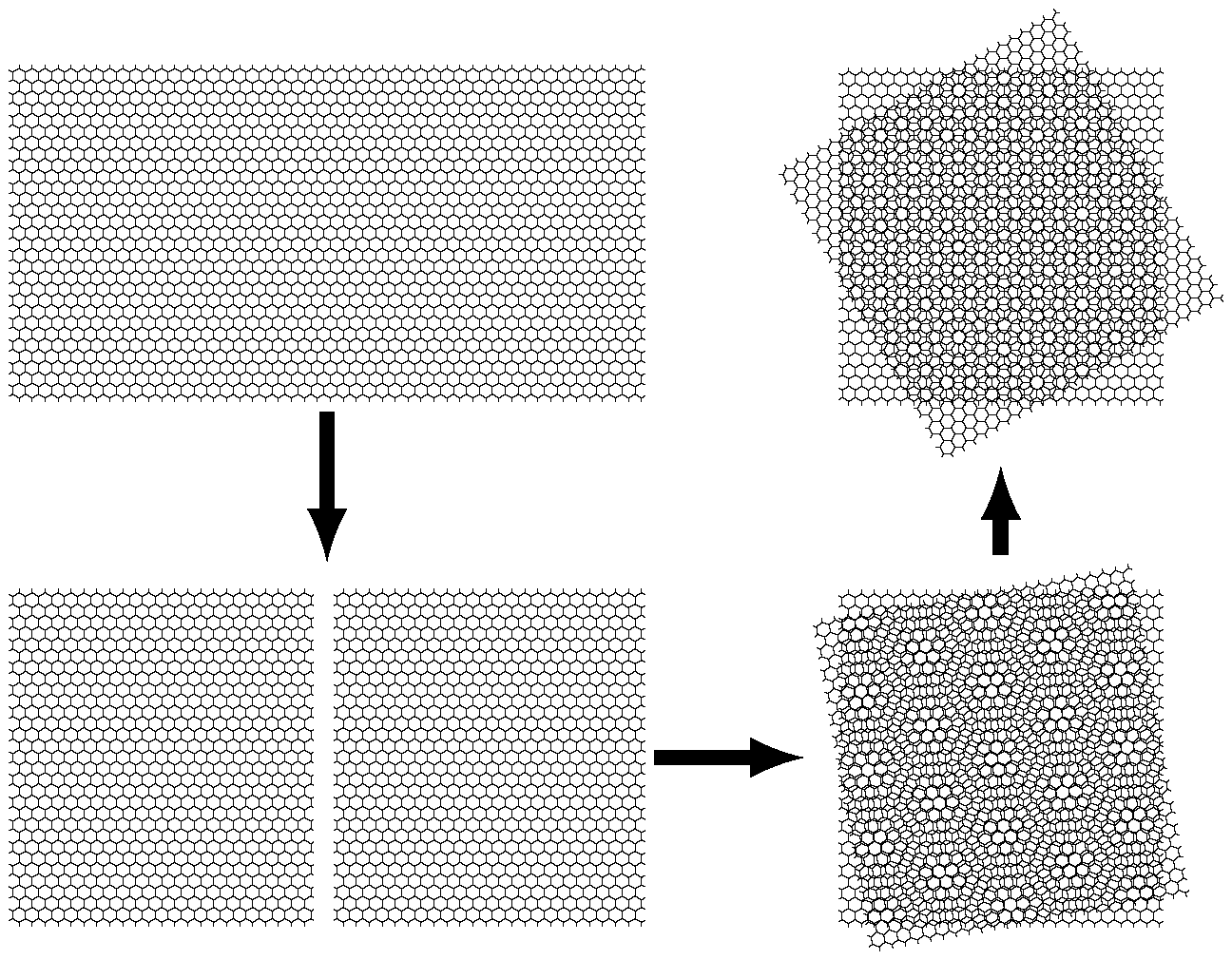
Graphene, a single atomic layer of graphite first found in 2004 [1], opened the new era of 2D materials. After more than a decade of intensive investigations, however, almost all novel properties of graphene have been studied. At the time when the heat wave of graphene research was about to pass, a groundbreaking paper published in 2018 [2] yet caused another wave. This time, the new finding is that via the so-called “tear-and-twist technique” (Figure 1), the resulting twisted bilayer graphene can be turned into an unconventional superconductor, when the twist angle is around 1.1 or 1.2 degrees, called magic angle. This shocked the entire condensed-matter physics community and caused an unprecedented upsurge in “twistronics” – whether theorists or experimentalists, people tried all kinds of twisted bilayer graphene with various twist angles. Soon it was found that the twisted bilayer graphene exhibits rather distinct behaviors depending on the twist angle. A new arena covering rather rich physics to be explored therefore emerged.
Roughly speaking, there are minimally-, small-angle-, magic-angle, and large-angle-twisted bilayer graphene. Among these, the large-angle-twisted bilayer graphene is what we want to slightly elaborate here. One of its special characteristics is the decoupling of the two layers of graphene. That is, the electric conduction between the two graphene layers is blocked, as if there is an insulating layer in between. This is somewhat hard to believe, but in a recent work [3] by Prof. Ming-Hao Liu of Department of Physics, in collaboration with the experimental group from ETH Zurich, a rather direct proof for this awkward behavior has been shown.
On the experiment side mainly conducted by Dr. Peter Rickhaus, two types of electron interferometers are fabricated, using two different types of bilayer graphene, one being two closely spaced sheets of graphene separated by an ultra-thin (~ 3.5 nm) insulator called hexagonal boron nitride (hBN), and the other being the large-angle twisted bilayer graphene without the intercalating hBN layer. In the interferometer, the bilayer graphene sample is sandwiched by a global back gate that covers the entire graphene sample and a local top gate that covers only the central region. The function of the gates is to tune the energy of electrons (and hence the wavelength that is inversely proportional to the energy). When the gate voltages are configured in a way that the carrier types of the inner and outer region are different, forming either an npn or pnp junction, the top-gated region functions as an electron resonance cavity, and the conductance of the device oscillates with the changing electron wavelength in the cavity. This is the basic working principle of the electron interferometer.
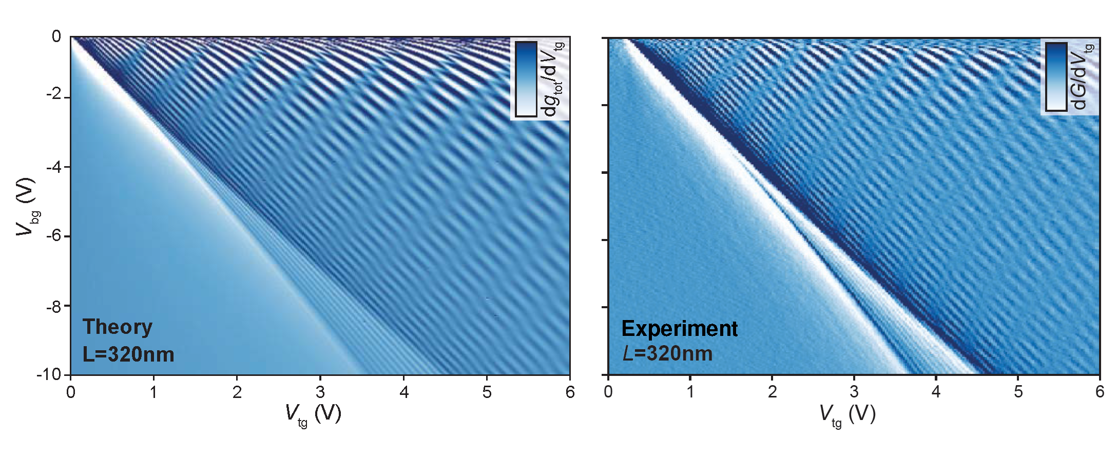
The two kinds of devices naturally show different results, but there are certain similarities. One of them is the separated low conductance dips when sweeping the global back gate. The low conductance comes from the vanishing density of states at the so-called Dirac point in the graphene energy band structure, above and below which carriers behave like electrons and holes, respectively. In the device with the intercalating hBN layer, the two individual sheets of graphene are gated with different efficiencies, such that the low-conductance points are revealed at different gate voltages. This is reasonably expected. In the device with the large-angle twisted bilayer graphene without the intercalating hBN layer, two slightly separated low-conductance points are also seen in the experiment, implying the decoupling of the two graphene layers. Assuming the two tightly spaced graphene layers to be electronically decoupled, Prof. Ming-Hao Liu constructed a rather efficient self-consistent quantum capacitance model and implemented the model into his quantum transport simulation, considering the same geometry as the device used in the experiment. The stunningly consistent results between the measurement and the simulation (Figure 2) provided a direct proof for the decoupling mechanism.
This exciting finding has many interesting implications. First, the structure of two conducting plates with an insulating layer in between is the simplest capacitor in electrostatics. The resulting capacitance is well-known to increase with the decreasing thickness of the insulator. The “insulating layer” for the case of decoupled twisted bilayer graphene is expected to be around the layer spacing of graphite: 0.334 nm, which is obviously thinnest ever for all capacitors. Secondly, the layer spacing plays a rather important role in the model of Prof. Liu. Interestingly, when using 0.334 nm, the transport simulation results in a conductance map that look also fine but a discrepancy between the measurement and simulation can be clearly seen. The best result shown in Figure 2 considered 0.12 nm as the spacing. The explanation is that the thickness of the insulating layer between the decoupled graphene layers is not the carbon-to-carbon distance but the remaining thickness when the electron cloud of the atomic orbitals is subtracted. This means that the thickness of graphene has been indirectly measured in such a transport experiment!
These cool findings opened up several directions to be further investigated, such as the effect of the applied magnetic field. This part has been taken over by Dr. Alina Mrenca-Kolasinska from Poland who joined the theory group of Prof. Liu to continue the collaboration with the group in ETH Zurich. The latest results have just been published very recently [4].
[1] K. S. Novoselov et al., Science 306, 666 (2004). [2] Y. Cao et al., Nature (London) 556, 43 (2018). [3] P. Rickhaus et al., Science Advances 6, eaay8409 (2020). [4] A. Mrenca-Kolasinska et al., 2D Mater. 9, 025013 (2022).
|
|||||||
|
Figure 1 Schematic of the “tear and twist” technique used to fabricate twisted bilayer graphene.
Figure 2 Theoretical (left) and experimental (right) results of the electron interferometer using large-angle twisted bilayer graphene [3]. |
|||||||
| ______________________________________________________________________________________________ | |||||||
|
|||||||
subscribe E-news
Vol.34 NO.1(2022.2)-5 Author information
|
Author
Associate Professor Ming-Hao Liu |
|
|
|
Research members Peter Rickhaus1, Ming-Hao Liu2, Marcin Kurpas3, Annika Kurzmann1, Yongjin Lee1, Hiske Overweg1, Marius Eich1, Riccardo Pisoni1, Takashi Taniguchi4, Kenji Watanabe4, Klaus Richter5, Klaus Ensslin1, Thomas Ihn1 1Solid State Physics Laboratory, ETH Zürich, CH-8093 Zürich, Switzerland. 2Department of Physics, National Cheng Kung University, Tainan 70101, Taiwan. 3Institute of Physics, University of Silesia in Katowice, 41-500 Chorzów, Poland. 4National Institute for Materials Science, 1-1 Namiki, Tsukuba 305-0044, Japan. 5Institute of Theoretical Physics, University of Regensburg, D-93040 Regensburg, Germany. |
|
Key words Graphene, quantum transport, twisted bilayer graphene |
|
Research areas Prospective science & technology research |
|
References Science Advances Vol. 6, no. 11, eaay8409 https://www.science.org/doi/10.1126/sciadv.aay8409 |
|
Dowonload |